
To address the pain points in the appearance inspection of wafer chipping and scratches, LuxMV has long focused on machine vision inspection for the semiconductor industry. By optimizing lighting solutions and imaging strategies, we deliver full-view high-definition imaging of wafers to clearly identify tiny defects, meeting the requirements for automated high-precision inspection.
The wafers under inspection in this case have typical defects including surface scratches, corner breakage and edge chipping. A comprehensive inspection of the solder side and overall appearance is required to detect all visible and hidden damages.
The original appearance of the workpiece is shown in the figure below:
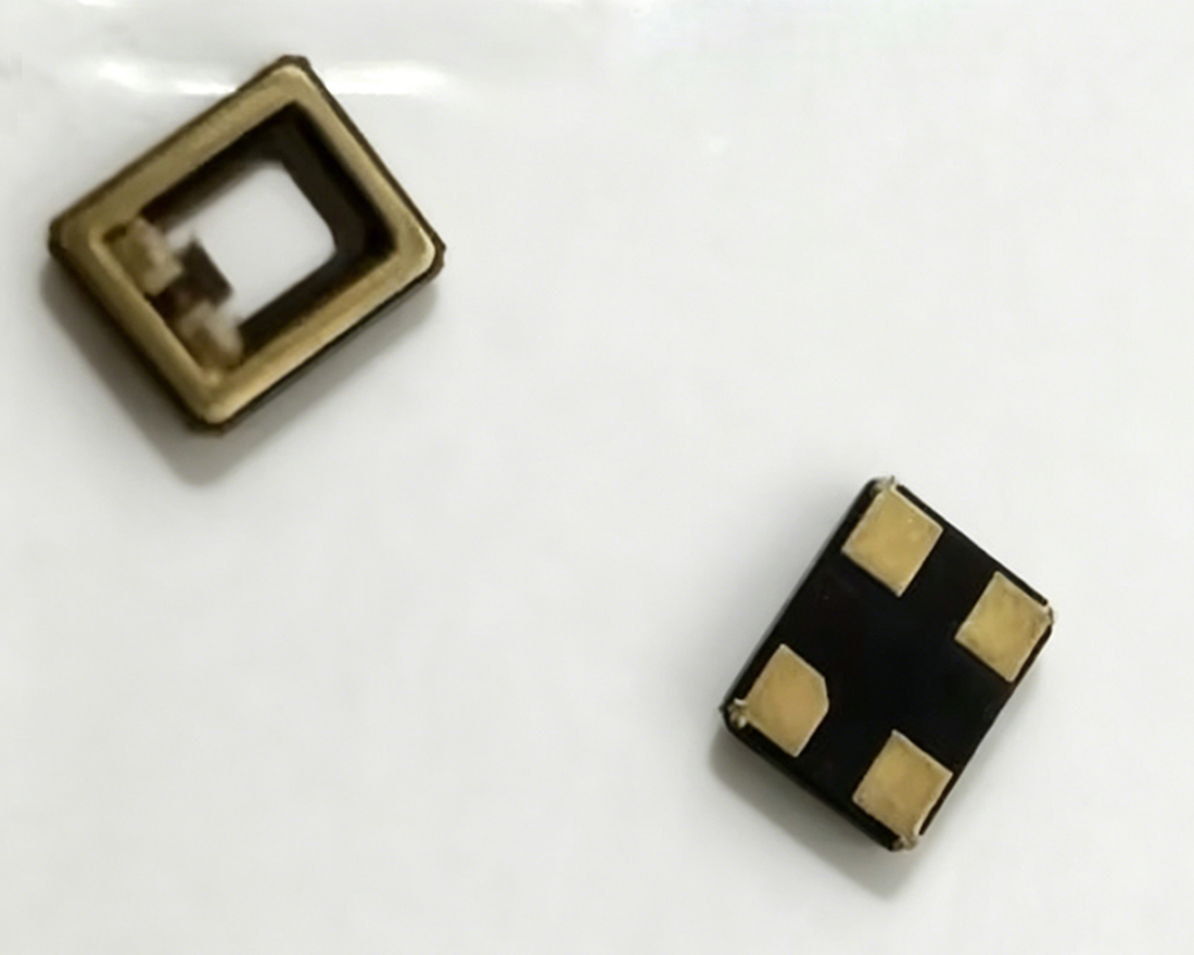 Workpiece 1
 Workpiece 2
The following factors shall be taken into consideration:
•Whether the surface of the test object is reflective, and whether defects present differences in brightness, shade or color.
•Whether the light emission angle can effectively suppress specular reflection and eliminate shadows and blind detection areas.
•After actual shooting and imaging, the contours of defects such as chipping and scratches are clear, with sufficient grayscale and color contrast against the base material.
•Compatibility with color industrial cameras and installation space is also required. The imaging quality shall be consistent, defects can be stably identified by vision algorithms, and the solution shall be applicable to mass production on production lines.
The light source selection is deemed feasible only when all the above requirements are met.
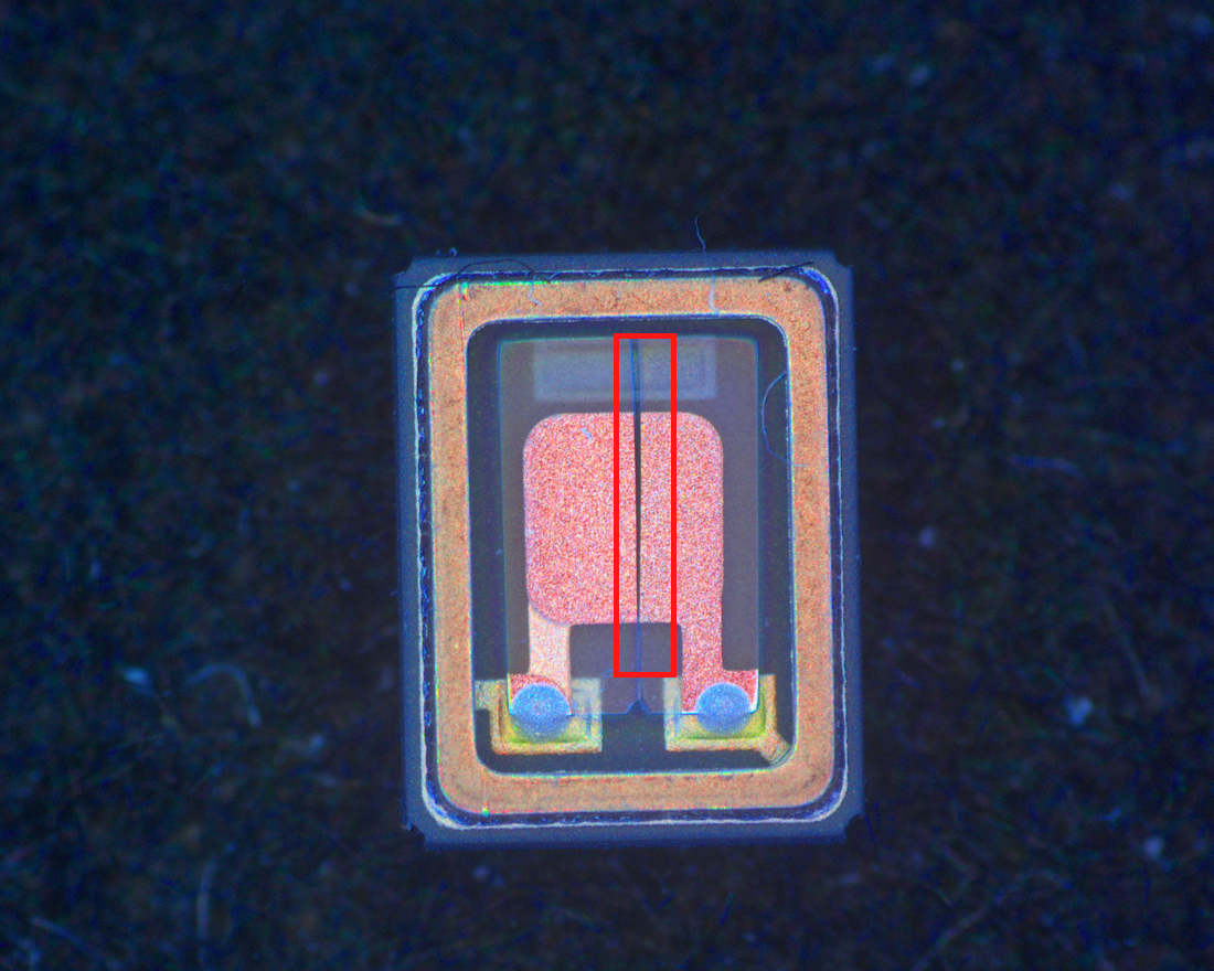
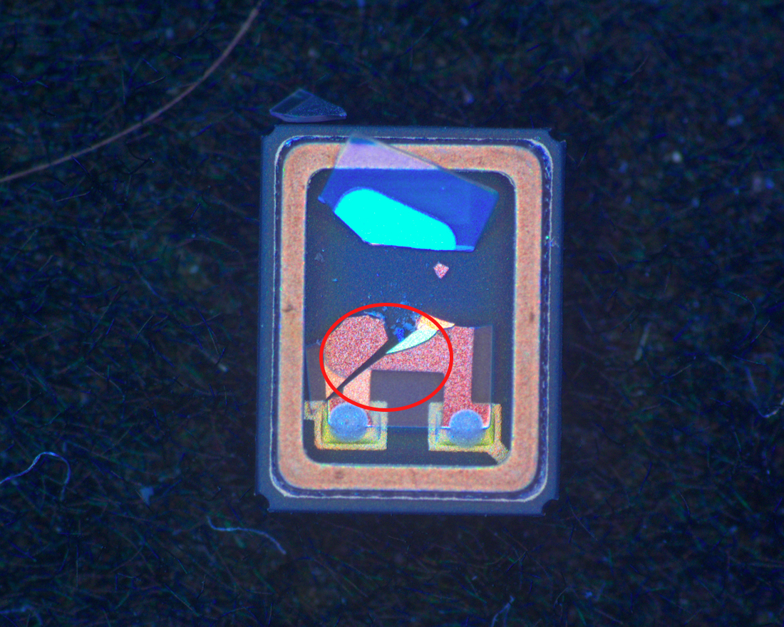
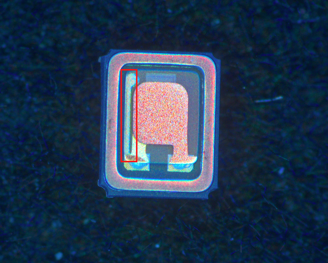
The imaging effect is as shown below:
 Cracked wafer
  Damaged wafer
 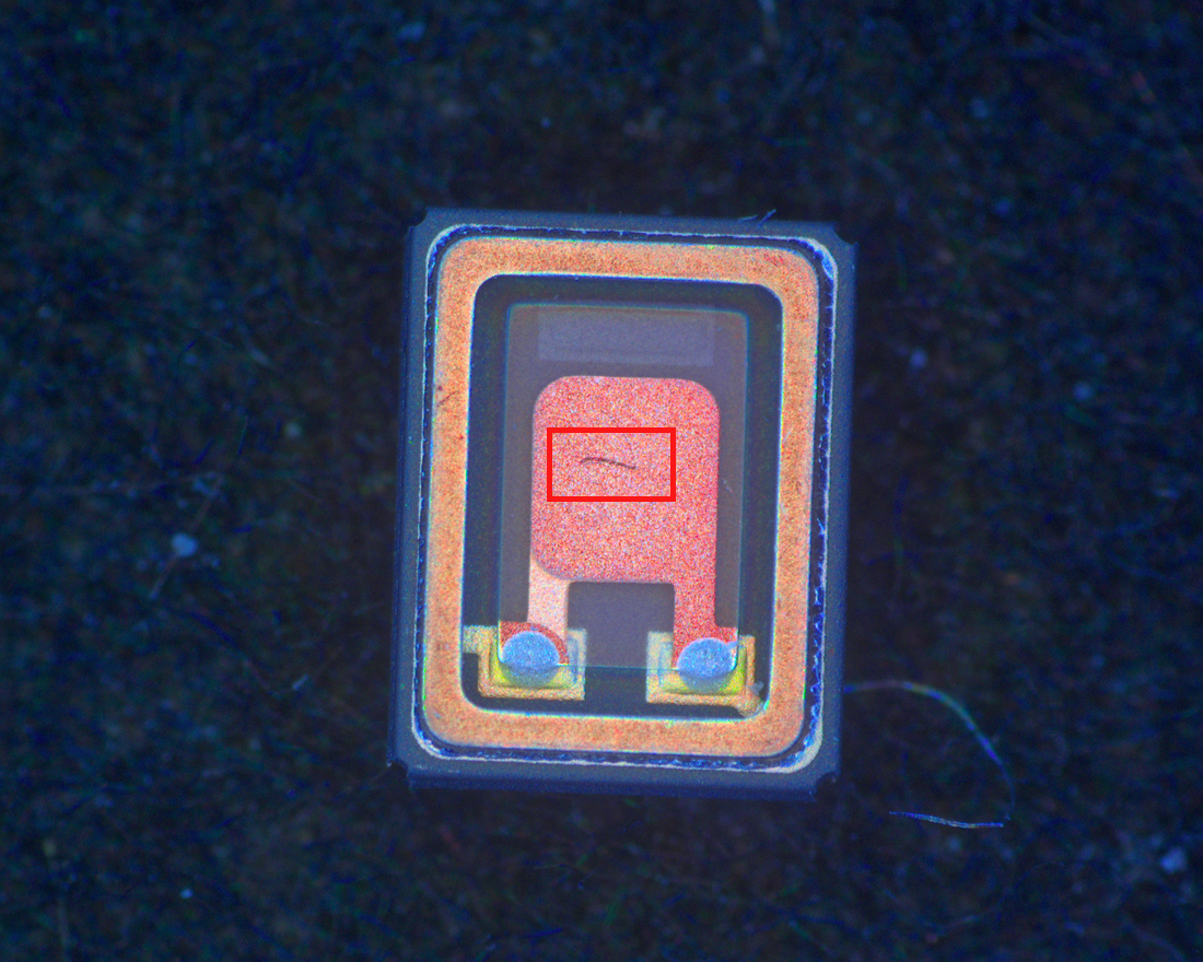 Foreign particles on the wafer
  Wafer scratch
•Cracks and damaged areas on the solder side of the wafer appear in distinct blue tones. Scratches and foreign matter on the front side also show unique color features.
•Leveraging rich color textures and chromatic aberration, qualified areas can be clearly distinguished from defective areas. This provides high-quality images for subsequent defect identification and analysis via machine vision algorithms.