
1.What is short-wave infrared light?
The light visible to our naked eyes (visible light) only occupies an extremely narrow segment of the electromagnetic spectrum (with wavelengths ranging from 380 to 780 nanometers). Short-wave infrared light (SWIR) is adjacent to the infrared band of visible light, with an industry standard wavelength range of 900 to 2500 nanometers. The professional description of its core characteristics is as follows:
1-1.Invisible but precisely detectable: Short-wave infrared light cannot be perceived by the naked eye, but through dedicated infrared sensors such as InGaAs (indium gallium arsenide), it can be converted into observable electrical signals and images, and the detection process will not cause any impact on the appearance or internal circuits of the chip (no light damage).
1-2.Excellent material penetration: It can efficiently penetrate key materials in semiconductor manufacturing - silicon wafers (especially with extremely high transmittance for wavelengths of 1100-1700 nanometers) and plastic packaging materials for chips (such as epoxy resin and polyimide), but cannot penetrate metals (such as copper and aluminum interconnection lines inside the chip), which is the core prerequisite for realizing the visualization of internal circuits.
1-3.Sensitivity of material properties: It has a unique absorption/reflection response to trace moisture, chemical bonds (such as epoxy bonds in packaging materials and oxidation bonds on wafer surfaces), and impurity content in materials. Different materials and defect states have significant differences in the reflectivity and absorption rate of short-wave infrared light, forming characteristic signals similar to "material fingerprints". It provides precise basis for defect identification - this feature is similar to the refraction difference of visible light by different materials, and normal structures can be distinguished from defects through signal differences.
2.How does short-wave infrared light achieve internal chip inspection?
Short-wave infrared light are not a single "light-emitting device", but rather form a complete detection module together with detection lenses, infrared sensors, and AI analysis systems. Their working principle can be divided into three core steps:
2-1.Penetrate the packaging layer and directly hit the core of the chip
Silicon wafers have a unique permeability to short-wave infrared light, especially at wavelengths of 1100-1700 nanometers, much like the high transmittance of visible light in glass (with a transmittance of over 80%). In contrast, the commonly used plastic packaging materials for chips (such as epoxy molding compound EMC) present a "semi-transparent" state within the wavelength range of 900-2000 nanometers. It allows short-wave infrared light to penetrate efficiently. On the contrary, the metal interconnection lines (copper wires, aluminum pads) and solder joints inside the chip will strongly reflect or absorb short-wave infrared light, forming a sharp contrast of light and dark with the surrounding packaging materials and silicon substrates, thus clearly presenting the shape of the internal lines in the imaging.
2-2.Multi-wavelength combination, covering all types of defect inspection
Short-wave infrared light can provide more characteristic wavelengths (industry commonly used 1050 nm, 1300 nm, 1550 nm, etc.), penetration and defect response characteristics of different wavelengths difference, need to be used according to the thickness of the encapsulation, defect type combination:
1050nm wavelength: It has a medium penetration ability and is suitable for thin package chips (package thickness < 500μm), which can clearly present the surface interconnection lines and solder joint morphology.
1300nm wavelength: It has strong penetration ability and is suitable for medium and thick packaged chips (packaging thickness 500μm-1mm), allowing it to penetrate the packaging layer to observe the bonding state between the chip core and the leads.
1550nm wavelength: It is highly sensitive to moisture and organic residues (such as photoresist residues after chip cleaning and impurities during the packaging process), and is mainly used to detect defects such as water vapor inside the package, cleaning residues, and contamination in the bonding zone. Through multiple scanning wavelength combination, which can realize on line breaking, solder joints virtual welding, packaging, water vapor bubbles embedded residue, impurities and other defects of comprehensive identification, to avoid a single wavelength detection blind area.
2-3.AI intelligent analysis enables efficient and precise judgment
Modern short-wave infrared detection systems, integrating machine vision and AI algorithms, do not merely present images. Instead, they first preset a standard image template of the normal structure of the chip, and then compare the real-time collected infrared images with the standard template at the pixel level. This enables precise identification of micrometer-level defects (the smallest recognizable defect size can reach 1-5μm, equivalent to 1/100 of the diameter of a human hair). It simultaneously achieves real-time feedback and automatic marking of problem areas, eliminating the need for manual visual comparison, significantly enhancing the efficiency and accuracy of detection.
3.Why is short-wave infrared light needed for chip inspection?
Traditional chip inspection methods (such as visible light imaging, manual visual inspection, and halogen lamp irradiation inspection) face three insurmountable professional challenges in modern high-density packaged chip inspection. The specific corrections are as follows:
3-1.Encapsulation penetration trap: Unable to penetrate the dense encapsulation layer
Modern chips (especially those for consumer electronics and automotive electronics) mostly adopt high-density plastic or ceramic packaging. The packaging layers are dense and relatively thick (typically ranging from several hundred micrometers to several millimeters), and visible light cannot penetrate the packaging layers, making it impossible to observe the internal circuits and bonding states. Even for thin-packaged chips, visible light can be scattered by the packaging material, resulting in blurred imaging and inability to identify subtle defects.
3-2.Thermal damage risk: Prone to damaging the delicate chip structure
In traditional detection, halogen lamps and incandescent lamps generate a large amount of infrared thermal radiation (mainly long-wave infrared) during the light emission process, with high heat generation and difficult temperature control. Moreover, the interconnection circuits, solder joints, and wafer cores inside the chip are extremely sensitive to temperature (exceeding 80℃ may cause thermal stress damage and solder softening). Long-term exposure can lead to performance degradation or even direct damage to the chip. It cannot meet the requirements of non-destructive testing of chips.
3-3.Efficiency and accuracy bottleneck: Unable to adapt to large-scale production
Manual visual inspection is not only slow (it takes tens of seconds to inspect a single chip), but also unable to identify micrometer-level defects, with extremely high rates of missed detection and false detection (usually exceeding 10%). Traditional visible light imaging inspection can only detect surface defects of chips and cannot cover internal defects, thus failing to meet the inspection requirements of modern large-scale and high-precision chip production (the inspection speed of chip production lines needs to reach several to dozens of chips per second).
Short-wave infrared light precisely address the above three major pain points: It can not only penetrate the packaging layer to achieve internal visualization, but also maintain low-temperature operation (no obvious thermal radiation during the light-emitting process, and the surface temperature of the light source can be controlled below 50℃), avoiding thermal damage to the chip. At the same time, combined with an AI system to achieve efficient and high-precision automatic detection, it has become an indispensable core component in modern chip manufacturing (especially in post-packaging detection and failure analysis).
As a professional manufacturer of visual light , we have been deeply engaged in the field of semiconductor testing and have developed a full range of short-wave infrared light products suitable for chip testing. Covering commonly used short-wave infrared light in the industry such as ring, coaxial, and backlight , as well as customized short-wave fiber infrared light for special detection scenarios in the semiconductor industry (such as micro-chips, high-density interconnect chips, and fiber-coupled detection), we can provide personalized light solutions based on the type of chip packaging and detection requirements, helping to improve the efficiency and accuracy of chip detection.
Short-wave fiber infrared light
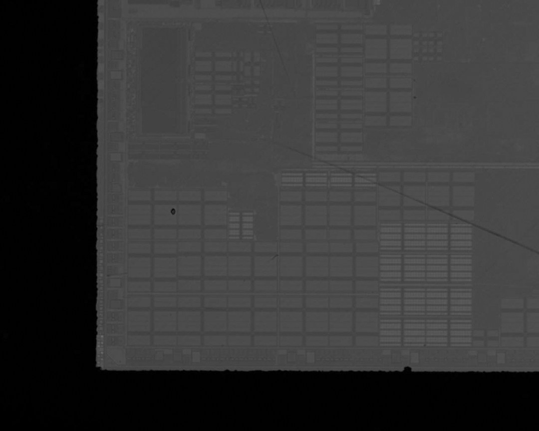
 SWIR 1300 spot light imaging
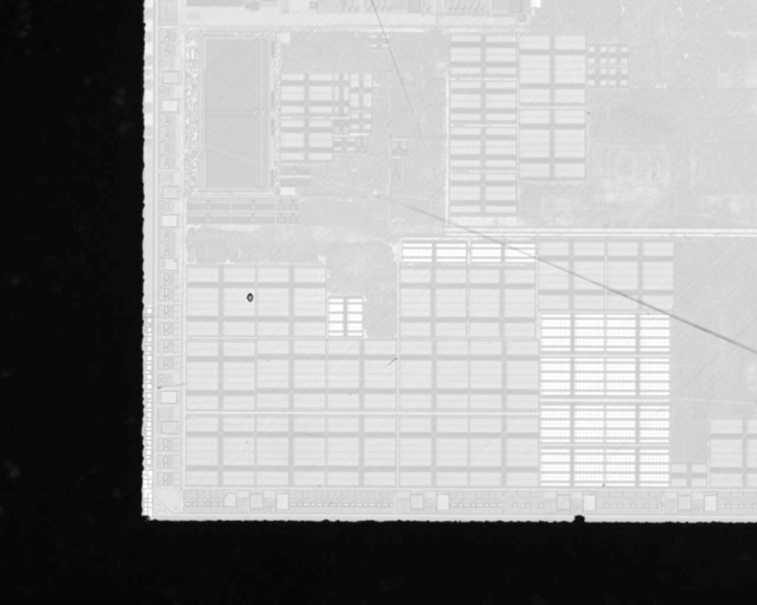
 SWIR 1300 fiber light imaging
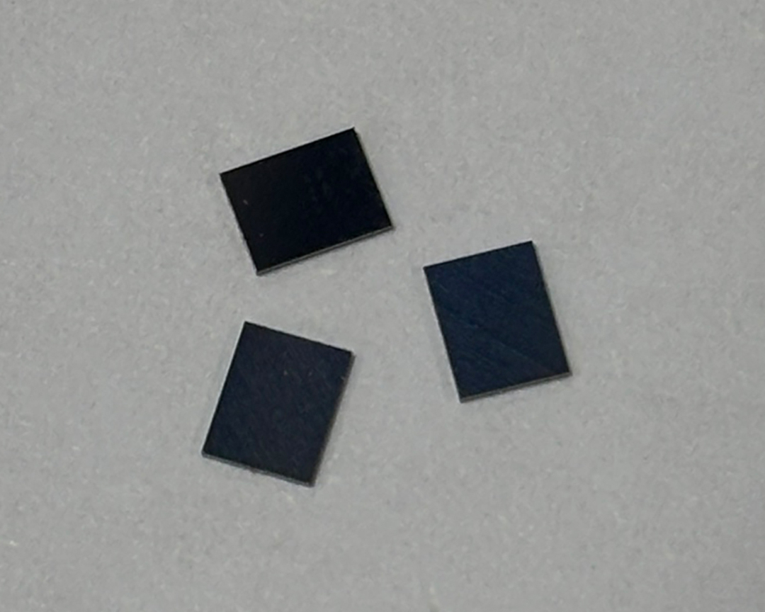
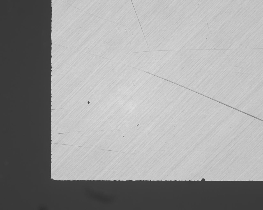
Now let's take a case to understand the imaging comparison of packaged chips under the irradiation of light of different wavelengths.
 object
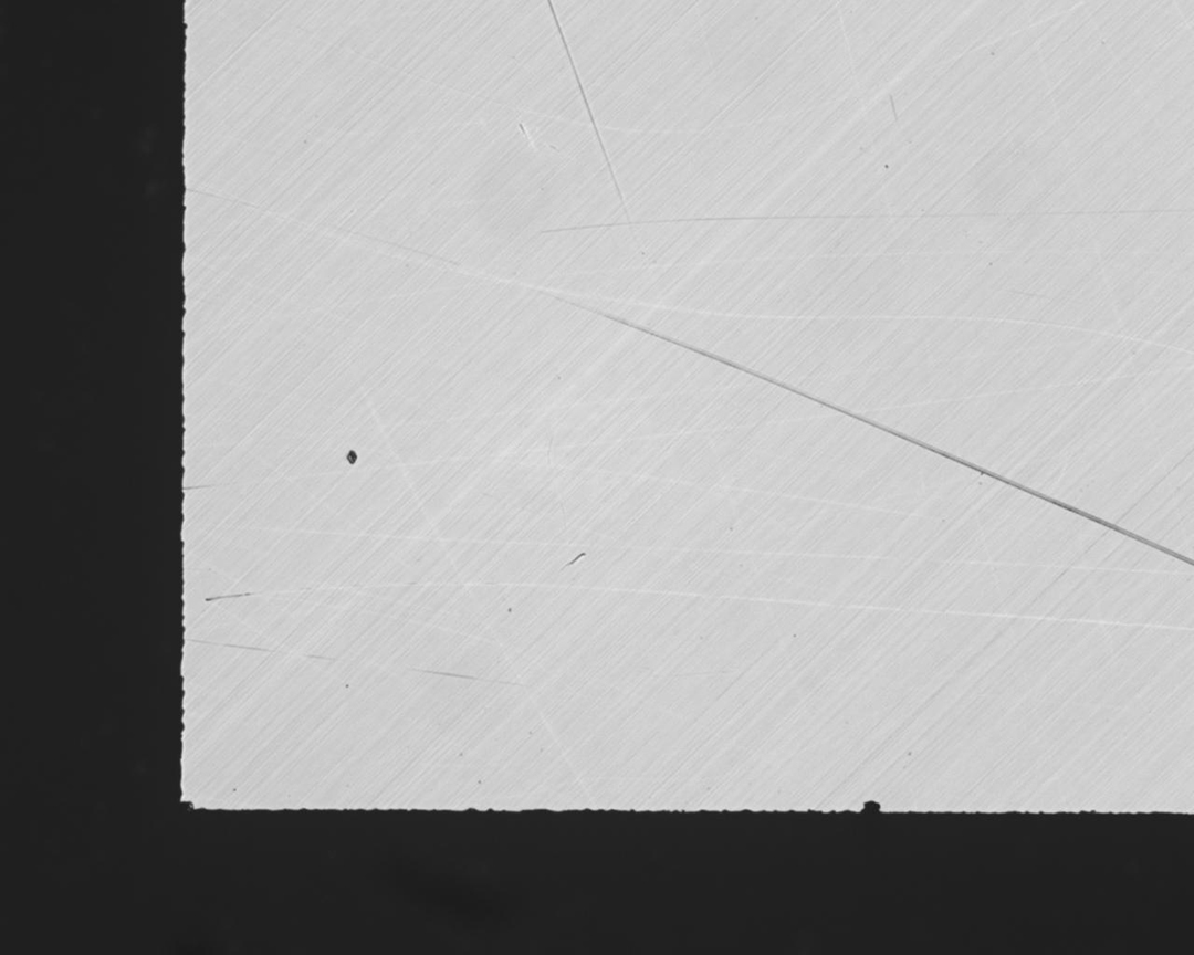 white light
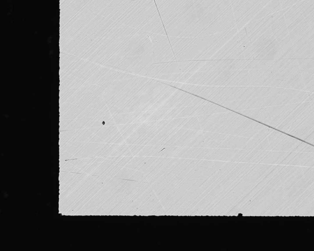 IR850nm
 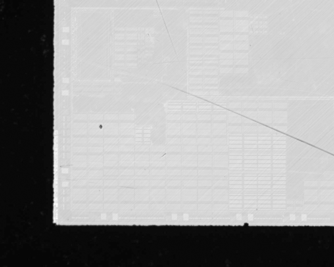 IR940nm
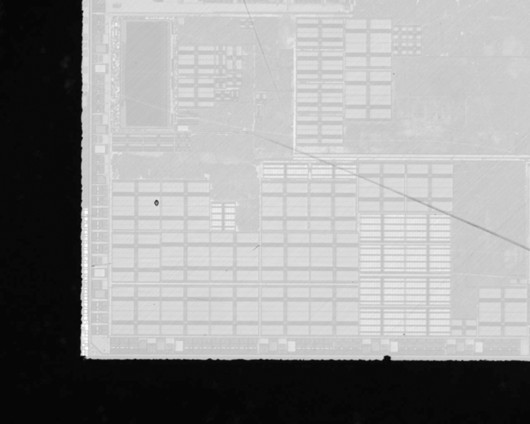 SWIR 1050nm
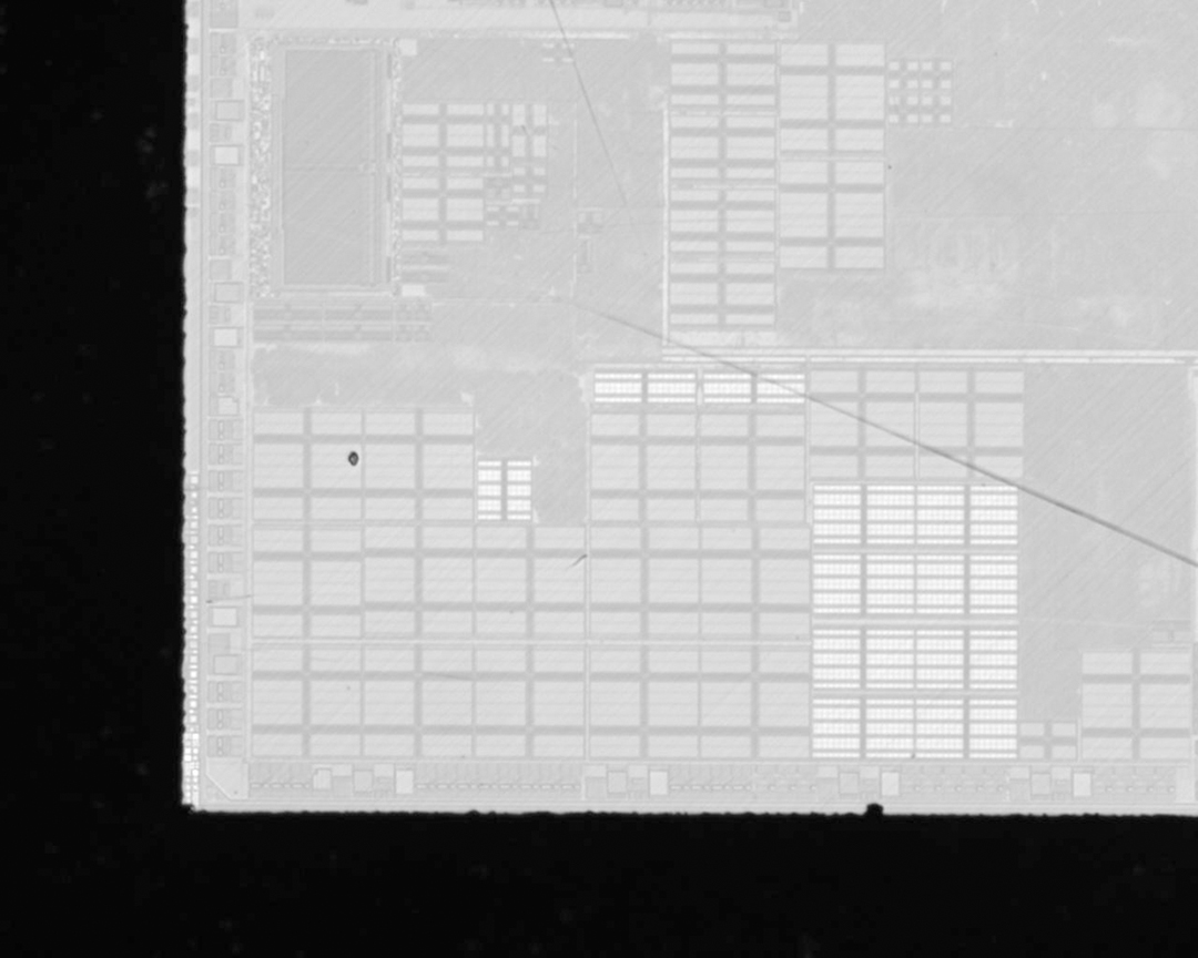 SWIR 1200nm
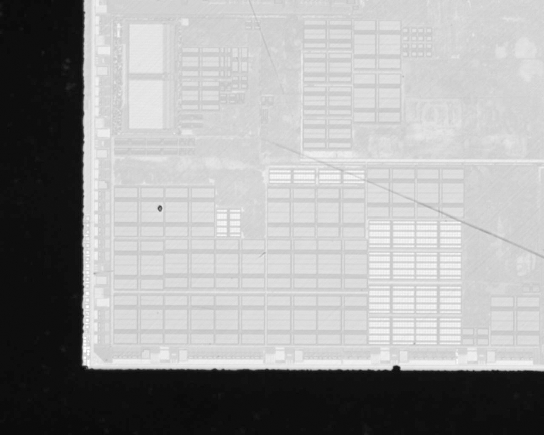 SWIR 1300nm
 SWIR1500nm
4.Future Expectations
With the continuous improvement of chip manufacturing processes and integration complexity, short-wave infrared technology will also undergo iterative upgrades. Higher resolution: from micron level towards nanoscale precision hyperfine precise matching chip manufacturing process needs.
Intelligent integration: Deeply integrated with the AI detection system to achieve intelligent prediction and efficient analysis of chip defects. Cost optimization: from high-end semiconductor manufacturing scene to the market gradually saturated, driving technology of large-scale popularization and fall to the ground.
5.Conclusion
Short-wave infrared light technology is becoming the core cornerstone of quality control in the semiconductor chip industry. With the high transparency feature of penetrating packaging, the precise ability of multi-wavelength scanning and the advantage of intelligent analysis and interpretation, it makes all kinds of hidden defects in chip production nowhere to hide, providing a guarantee for the high reliability of chip products. With the continuous evolution of technology, its comprehensive improvement in detection resolution, intelligent integration and cost-effectiveness will further drive quality innovation in the semiconductor manufacturing field and help the industry develop towards higher processes and higher integration.