
This technical note explains how LuxMV applies semiconductor methods to improve image contrast, reduce optical uncertainty, and support repeatable machine vision inspection.
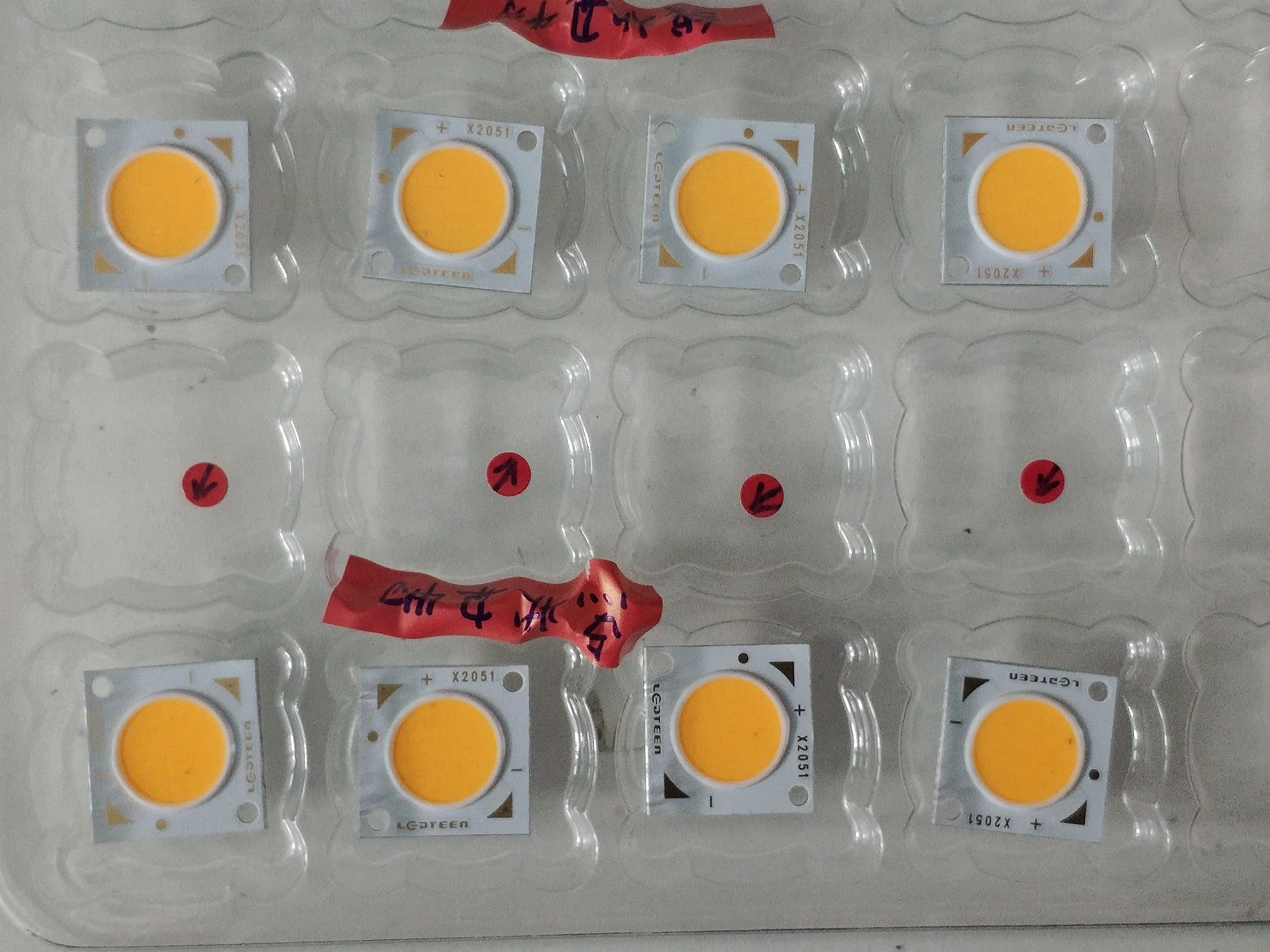
Inspection Challenge
The main engineering challenge is not only brightness. The light must create useful contrast for the inspected feature while keeping exposure, working distance, heat, and mechanical integration within the limits of the production station.
Lighting Approach
A robust LuxMV setup starts with sample testing. Engineers compare illumination angle, wavelength, diffusion, and controller timing while keeping the camera, lens, and part position stable. The final recipe is selected by measured contrast margin rather than by visual preference alone.
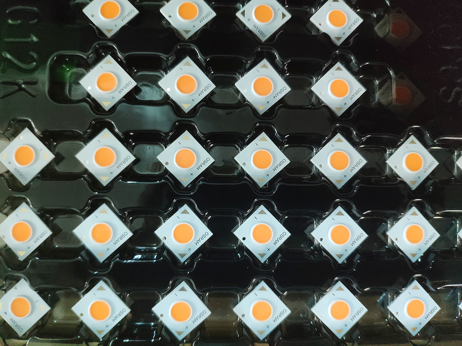
Where This Method Fits
Typical applications include automated defect detection, OCR or mark reading, contour measurement, reflective-surface inspection, and quality control for parts whose appearance changes with material, coating, color, or process conditions.
- Use controlled illumination to separate the target feature from background texture.
- Validate the image under real line speed, exposure, and trigger constraints.
- Keep enough contrast margin for normal material and process variation.
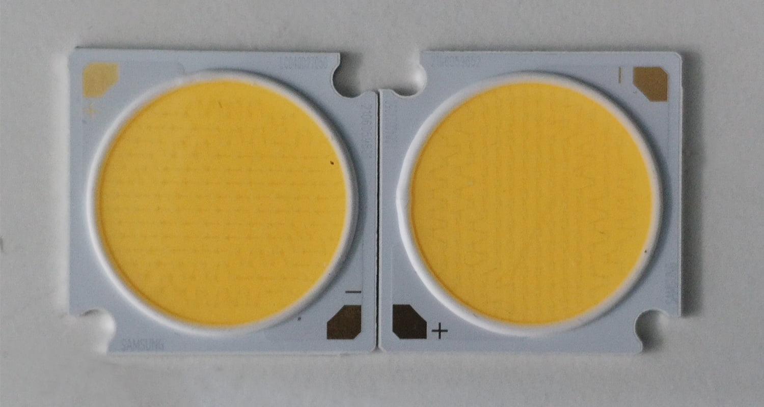
LuxMV Engineering Notes
For production use, document the selected light model, exposure time, gain, aperture, working distance, trigger timing, and any polarizer or diffuser used in the optical path. This makes the inspection easier to reproduce when part suppliers, surface finish, or line speed changes.